


Focused Research Analysis at Your Finger Tips
UW-Stout's Analysis Lab is a premier facility designed to enhance students' understanding of nanoscience and applied physics through hands-on learning and advanced research. This lab is equipped with state-of-the-art instruments that enable detailed characterization and analysis of various materials, making it an invaluable resource for students and research groups alike.
Key instruments in the Analysis Lab include the Scanning Electron Microscope (SEM) and the Atomic Force Microscope (AFM). The SEM uses electrons to produce high-resolution images and perform energy-dispersive X-ray spectrometry, essential for materials characterization and microanalysis. The AFM provides detailed surface topography measurements at the nanoscale, utilizing Van der Waals forces to examine even the smallest features of a sample. These cutting-edge tools enable comprehensive exploration and innovation in nanoscience, ensuring students gain practical skills and experience critical for their future careers in research and industry.
Degrees That Do More in This Lab
Dive Deeper Into the Analysis Lab's Equipment
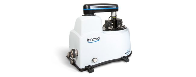
The Atomic Force Microscope (AFM) provides a three-dimensional surface profile of a sample at the nanoscale by using a mechanical probe to scan the surface. This allows for the study of surface topography and properties with extremely high resolution, essential for nanotechnology and materials science.
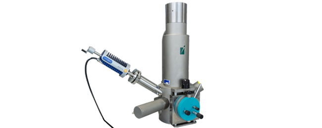
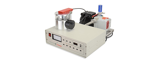
The Carbon Coater applies a fine layer of carbon to samples, which is particularly useful for preparing specimens for both SEM and EDS analysis. This coating method is critical for reducing charging effects and improving image clarity and elemental analysis accuracy.
The Energy-Dispersive X-ray Spectrometer (EDS) is integrated with the SEM and uses X-rays generated by electron interactions to analyze and identify the elemental composition of samples. This technique is essential for detailed material characterization and understanding chemical compositions.
The Scanning Electron Microscope (SEM) uses a focused beam of electrons to create high-resolution images of a sample's surface, revealing fine details not visible with traditional microscopes. It also performs energy-dispersive X-ray spectrometry (EDS) to determine the elemental composition of materials.
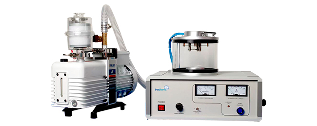
The Sputter Coater is used to coat samples with a thin layer of conductive material, typically gold or carbon, before SEM analysis. This coating enhances the imaging quality by preventing charge buildup on non-conductive samples.